
New Nanostructure Could Be The Key To Quantum Electronics
Eddie Gonzales Jr. – MessageToEagle.com – A novel electronic component from TU Wien (Vienna) could be an important key to the era of quantum information technology: Using a special manufacturing process, pure germanium is bonded with aluminum in a way that atomically sharp interfaces are created.
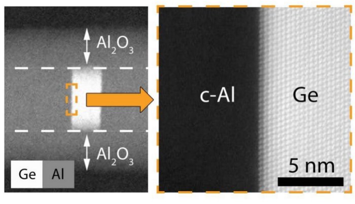 Extremely precise interface between the two materials. Credit: Vienna University of Technology
This results in a so-called monolithic metal-semiconductor-metal heterostructure.
This structure shows unique effects that are particularly evident at low temperatures. The aluminum becomes superconducting—but not only that, this property is also transferred to the adjacent germanium semiconductor and can be specifically controlled with electric fields. This makes it excellently suited for complex applications in quantum technology, such as processing quantum bits. A particular advantage is that using this approach, it is not necessary to develop completely new technologies.
Instead, mature and well-established semiconductor fabrication techniques can be used to enable germanium-based quantum electronics.
Germanium: difficult to form high-quality contacts
“Germanium is a material which is acknowledged to play an important role in semiconductor technology for the development of faster and more energy-efficient components,” says Dr. Masiar Sistani from the Institute for Solid State Electronics at TU Wien. “However, if one intends to use it to produce components on a nanometre scale, you run into a major problem: it is extremely difficult to produce high-quality electrical contacts, because even the smallest impurities at the contact points can have a major impact on the electrical properties. We have therefore set ourselves the task of developing a new manufacturing method that enables reliable and reproducible contact properties.”
Traveling atoms
The key to this is temperature: when nanometre-structured germanium and aluminum are brought into contact and heated, the atoms of both materials begin to diffuse into the neighboring material—but to very different extents: the germanium atoms move rapidly into the aluminum, whereas aluminum hardly diffuses into the germanium at all. “Thus, if you connect two aluminum contacts to a thin germanium nanowire and raise the temperature to 350 degrees Celsius, the germanium atoms diffuse off the edge of the nanowire. This creates empty spaces into which the aluminum can then easily penetrate,” explains Masiar Sistani. “In the end, only a few nanometre area in the middle of the nanowire consists of germanium, the rest has been filled up by aluminum.”
Normally, aluminum made up of tiny crystal grains, but this novel fabrication method forms a perfect single crystal in which the aluminum atoms are arranged in a uniform pattern. As can be seen under the transmission electron microscope, a perfectly clean and atomically sharp transition is formed between germanium and aluminum, with no disordered region in between. In contrast to conventional methods where electrical contacts are applied to a semiconductor, for example by evaporating a metal, no oxides can form at the boundary layer.
Feasibility check in Grenoble
In order to take a closer look at the properties of this monolithic metal-semiconductor heterostructure of germanium and aluminum, Masiar Sistani collaborated with Prof. Olivier Buisson’s quantum engineering group at the University of Grenoble. It turned out that, the novel structure indeed has quite remarkable properties:
“Not only were we able to demonstrate superconductivity in pure, undoped germanium for the first time, we were also able to show that this structure can be switched between quite different operating states using electric fields,” reports Dr. Masiar Sistani. “Such a germanium quantum dot device can not only be superconducting but also completely insulating, or it can behave like a Josephson transistor, an important basic element of quantum electronic circuits.”
This new heterostructure combines a whole range of advantages: The structure has excellent physical properties needed for quantum technologies, such as high carrier mobility and excellent manipulability with electric fields, and it has the additional advantage of fitting well with already established microelectronics technologies: Germanium is already used in current chip architectures and the temperatures required for heterostructure formation are compatible with mature semiconductor processing schemes.
“We have developed a structure that not only has theoretically interesting quantum properties, but also opens up a technologically very realistic possibility of enabling further novel and energy-saving devices,” says Dr. Masiar Sistani.
Written by Eddie Gonzales Jr. MessageToEagle.com Staff
Related Posts
-
 ‘Breath’ Between Atoms – A New Building Block For Quantum Technology
-
 Stable Qubit – A Prime Candidate For Universal Quantum Computer
-
 UBCO Study Debunks The Idea That The Universe Is A Computer Simulation
-
 The Inner Workings Of Quantum Computers – Revealed
-
 Physicists Trap Electrons In A 3D Crystal For The First Time
-
 Recent Developments In Quantum Chromodynamics – Examined
-
 Mysteries Of The Universe Under The Skin Of An Atomic Nucleus – Revealed
-
 Anomaly Confirmed: Experiment Results Point To New Elementary Particle
-
 Entanglement Unlocks Scaling For Quantum Machine Learning
-
 Strange New Phase Of Matter Created In Quantum Computer Acts Like It Has Two Time Dimensions